
Abstract
Given the significance of microwave filters in real-world systems and the wide variety of potential applications, the domain of microwave filter design has been overgrowing. Modern computer-aided design (CAD) software based on the insertion loss approach is used for the majority of microwave filter designs. Microwave filter design is still a topic of active research due to ongoing developments in distributed element network synthesis, the use of low-temperature superconductors and other novel materials, and the integration of active devices in filter circuits.
This report discusses the design and analysis of a third-order Tchebyshev low-pass microstrip filter. The prototype filter and the lumped element filter with a cut-off of 2.5 GHz and characteristic impedance of 50 Ω are designed using standard formulas. The design and simulation of the low-pass filter are performed on CST Studio software. After the simulation, the final component is fabricated using Fr 4 substrate with er = 4.3 and thickness h = 0.8 mm and then tested using Vector Network Analyzer. The practical simulation and the measured results are reported and show a good agreement together.
Introduction
The filter is a device used to control the frequency response. Typical frequency responses include low-pass, high-pass, bandpass, and band-reject characteristics. A filter that allows low-frequency signals and rejects high-frequency signals, and transmits low-frequency signals from the input to the output port with minimum attenuation is called a low-pass filter. The amount of attenuation depends on the type of filter. The Low pass Chebyshev filter, made with LC combinations (Inductor and Capacitor), provides a faster transition from passband to stopband and has more ripples in the pass band.
The Microstrip line is used for designing the filter as it is easy to fabricate and has low insertion loss. The microstrip line sections are equivalent to Inductors and Capacitors, and to obtain a filter with the desired cutoff frequency, length and width parameters are calculated. After getting the required specifications, the filter structure has been designed with the help of CST Studio. This is software used for designing, analyzing, and optimizing electromagnetic Components and Systems. The dxf files obtained from the design were imported into the Design Pro software
And used for fabrication.
Literature Review
A number of research papers have been published on the design, simulation, and fabrication of low-pass filters using different software and design techniques. This review provides a brief overview of research papers relevant to the project title.
- Saxena, Shefali & Porwal, Shikha & Soni, Komal & Chhawchharia, Pradeep. (2009). Design and Analysis of Chebyshev Low Pass Filter using Insertion Loss Method.
- This paper discusses the use of the insertion loss method for the design and analysis of a 5th Chebyshev low-pass filter with a cutoff frequency of 2.5 GHz, characteristic impedance of 50 Ω, and passband ripple of 0.01 dB.
- PUFF software is used to simulate the lumped element filter, and the results are examined.
- The lumped element filter is then converted into a planar filter, and Micro-stripes software is used for its simulation and analysis.
- The microstrip is fabricated using GML100 substrate with er =3.2 and thickness h = 0.762 mm.
- The optimized low pass filter with end correction shows a measured cutoff frequency of 2.68 GHz and an impedance bandwidth of 2.82 GHz.
- Due to lead inductance and stray capacitance, the cutoff frequency of distributed and lumped elements exhibits a 700 MHz variance during analysis.
- R. Chaurasia, Mukesh & Raval, Falguni. (2016). Third Order Low Pass Chebyshev Filter Characteristic Realization Using the Ansoft Designer.. Inventi Impact - Antennas & Propagation. 2016. 1-4.
- This paper reports the design of a third-order low-pass Chebyshev filter with a cutoff frequency of 1 GHz and having a 1dB passband ripple.
- The lumped parameter filter is simulated in ANSOFT DESIGNER.
- The stepped impedance method is used to obtain the Microstrip filter, and the microstrip design and analysis are carried out using Fr 4 epoxy as substrate in ANSOFT HFSS.
- An insertion loss of -3.14 dB is obtained at 1.09 GHz for lumped network low pass filter design, and an insertion loss of -3.19 dB at 1.05 GHz for microstrip low pass filter design.
- Sheetal (2015). Stepped Impedance Microstrip Low-Pass Filter Implementation for S-band Application.
- This paper discusses the design of an S-band low pass filter using microstrip technology operating at 2.5 GHz for permittivity 4.1 with a substrate of thickness 1.6 mm and order n=6.
- The filter is designed using AWR microwave office simulation software, and the design and optimization of the lowpass filter is done using microstrip lines.
- The lowpass filter is then fabricated using photolithographic process and tested using vector network analyzer.
- The cutoff frequency obtained is lower than the desired value of 2.5 GHz, which may be due to imperfect fabrication and connection of SMA connector.
Methodology
In order to create practical filters, the lumped component filters must be transformed into distributed elements. In the design of microwave filters, we are mainly faced with two problems. The first is that only lumped parts function correctly within the constrained frequency range. The second is that while operating at microwave frequencies, there is no insignificant space between components. In order to turn lumped parts into transmission line sections, Richard’s transforms are utilized to solve the first issue. Using transmission elements to separate filter elements, Kuroda’s identities can be utilized to solve the second issue.
The design of low-pass filters involves two steps:
- The first step is to choose the appropriate type of response and order of the filter based on the desired specifications. The lowpass prototype filters’ element values are normalized to have a source impedance of gO = 1 and a cutoff frequency of wc = 1. They are then transformed to obtain the L-C elements for the required cutoff frequency and the source impedance.
- The next step is to find an appropriate microstrip realization that approximates the lumped element filter. The filter is then fabricated for a normalized cutoff frequency of wc on an Fr4 substrate with permittivity er and thickness h mm.
The filter design steps are as follows:
1) Filter specifications:
Passband: lowpass
Relative Dielectric Constant $\epsilon_r$ = 4.3
Height of substrate $h$ = 0.8 mm
Cutoff frequency = 2.5 GHz
The filter impedance $Z_o$ = 50 Ω
The highest line impedance $Z_H$ = $Z_{OL}$ = 120 $\Omega$
The lowest line impedance $Z_L$ = $Z_{OC}$ = 20 $\Omega$
2) Order of the filter:
For normalized LPF design with source impedance $g_0 = 1$ and cut-off frequency $w_c = 1$, the elemental values for equal-ripple low-pass filter prototypes are tabulated in table 1 for N=1 to N=10.
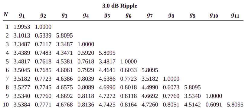
Table 1: Element values for Equal-Ripple low-pass filter prototypes ( $g_0=1$ , $w_c = 1$, N=1 to N=10, 3.0 dB ripple)
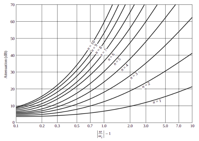
Figure 1: Attenuation characteristics for various N values versus normalized frequency.
Since the order of the filter needed is N = 3, we obtain the following filter element coefficients -
| $g_0 = R_s$ | $g_1 = L_1$ | $g_2=C_2$ | $g_3 = L_3$ | $g_4 = R_L$ |
|---|---|---|---|---|
| 1.000 | 3.3487 | 0.7117 | 3.3487 | 1.000 |
The actual values of the inductance Li and capacitance Ci can be calculated from the equations:
\[L_i = Z_0 g_i/2\pi f_c \newline C_i = g_i/Z_02\pi f_c\]The electrical length of the inductor
\[\beta l = LZ_0/Z_H\]The electrical length of the capacitor
\[\beta l = CZ_L/Z_0\]The L and C values are the normalized element values of the low pass prototype.
The width of the high impedance line assuming $w/h \leq 2$ and $w/h \geq 2$ can be calculated using the formulas -
\[\frac{W}{d}= \begin{cases}\frac{8 e^A}{e^{2 A}-2} & \text { for } W / d<2 \\ \frac{2}{\pi}\left[B-1-\ln (2 B-1)+\frac{\epsilon_r-1}{2 \epsilon_r}\left\{\ln (B-1)+0.39-\frac{0.61}{\epsilon_r}\right\}\right] & \text { for } W / d>2\end{cases}\]where
\(\begin{aligned} & A=\frac{Z_0}{60} \sqrt{\frac{\epsilon_r+1}{2}}+\frac{\epsilon_r-1}{\epsilon_r+1}\left(0.23+\frac{0.11}{\epsilon_r}\right) \\ & B=\frac{377 \pi}{2 Z_0 \sqrt{\epsilon_r}} . \\ & \sqrt{\varepsilon_e} k_0 l=\beta l=\frac{L R_0}{Z_n}=\frac{C z_L}{R_0} \end{aligned}\) where $k_0=2 \frac{\pi f}{c}, c=3 \times 10^8$ and \(\varepsilon_e=\frac{\varepsilon_R+1}{2}+\frac{\varepsilon_R-1}{2} \frac{1}{\sqrt{1+\frac{12 d}{w}}}\)
3) Dimensions of the filter:
The following are the dimensions of the filter, calculated using the formulas mentioned above -
| l0 | 5 mm | W0 | 1.5559 mm |
|---|---|---|---|
| l1 | 9.35 mm | W1 | 0.5 mm |
| l2 | 3.21235 mm | W2 | 5.62716 mm |
| l3 | 9.35 mm | W3 | 0.5 mm |
| l4 | 5 mm | W4 | 1.5559 mm |
The values of $L_0$ and $L_4$ were chosen to be 5 mm so that the total length of the feedline, which is equal to 31.91235 could be close to $\lambda / 4$, which is equal to 30 mm for 2.5 GHz frequency.
4) Design of the filter:
CST Studio software has been used for the design and simulation of the low-pass filter. The following picture shows the schematic -
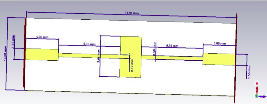
Figure 2: Schematic of microstrip filter with dimensions.
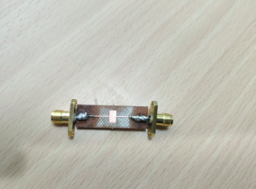
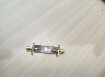
5) Fabrication:
The dxf files obtained from designing the low-pass filter prototype on CST Studio were used for the fabrication process. The dxf files were imported into the Design Pro software which is used for generating milling outlines, rubout, and contour routing. The Design View software is then used to fabricate boards with the desired design on a plate comprised of the substrate material and a copper layer.
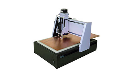
Figure 3: MITS PCB Machine
6) Analysis:
After obtaining the microstrip of the desired specifications, ports are soldered on each side, and the response of the fabricated low-pass filter is measured on a Vector Network Analyzer (VNA).
Design and Simulation
1) Design
The software used for the design and simulation of the filter was CST (Computer Simulation Technology) Studio which is an electromagnetic wave analysis software. The software offers multiple templates across the EM spectrum, the ‘Microwave and RF/Optical’ template was used for designing the planar microstrip line filter in the frequency domain.
Since the goal was to study the losses/ reflection, E-filed, H-field, Power loss were the parameters chosen for monitoring. Since the cut-off frequency was 2.5 GHz, the frequency range selected for modeling and analysis was 1.5-3GHz. The design procedure was as follows:
- First the bottom layer of the filter, that is, the ground plane was inserted [material from library: copper (lossy)] and dimensions were specified according to the calculations shown in the Methodology section.
- This was followed by the substrate layer made of FR4 substrate with Ɛr = 4.3. These two were added as separate elements.
- Next, the feedline layer was modeled, using copper(lossy). The 4 feedline parts were added in accordance to dimensions specified in the Methodology section. During the simulation, they were added as different elements. While fabrication, it was learnt that a better design strategy is to model the entire feedline as a single component.
- To simulate and study the s-parameters, port definition was required. The ports were created by using the face pick tool and the port extension coefficient calculator under macros solver. After this the simulation was run.
The following is the model designed in CST studio:
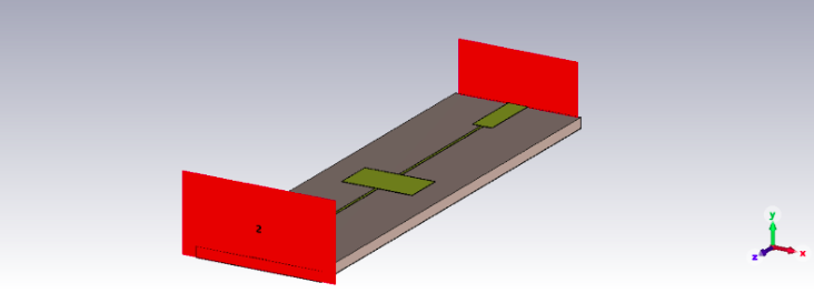
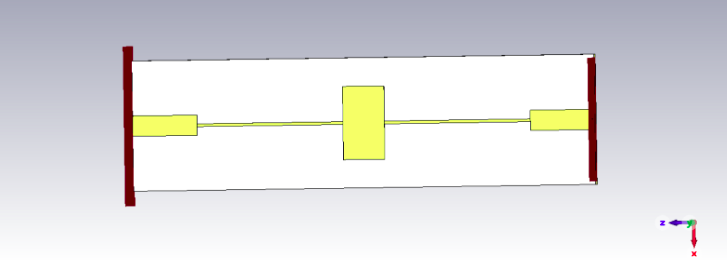
Figure 5: Microstrip filter model
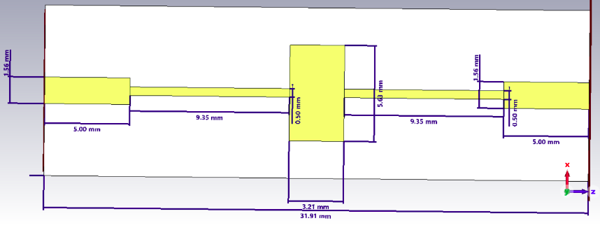
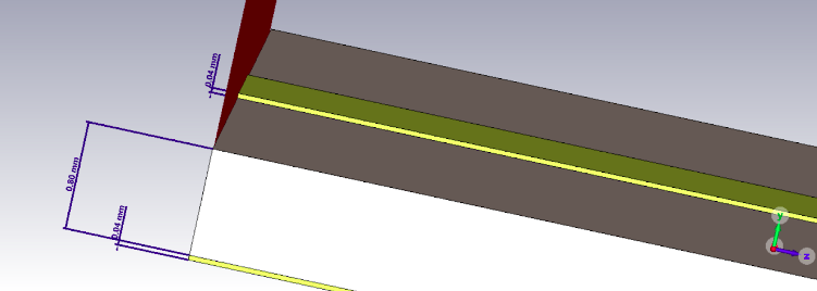
Figure 6: Microstrip filter schematic with dimensions
2) Simulation and s-parameter analysis
Once the simulation is run, the circuit can be analyzed through s-parameters (scattering parameters). S-parameters are network analysis parameters used for microwave circuits since it is not feasible to measure z-, abcd, h- parameters for RF circuits. Since the circuit under consideration is a low pass filter, which is a 2-port device, its s-parameters can be represented through a 2x2 reciprocal matrix.
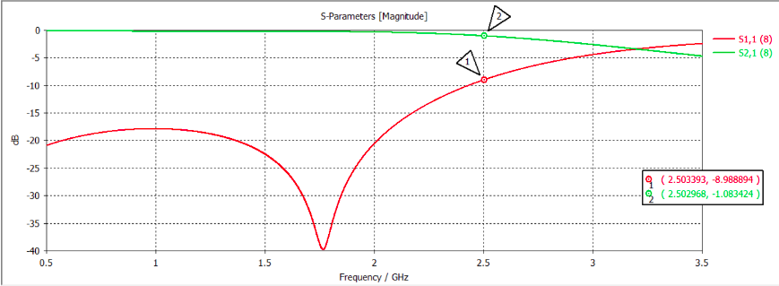
Figure 7: s-parameter results from CST Studio
The S11 parameter represents the return loss/ reflection coefficient of the transmission line. The ideal value of this parameter for a good transmission should be -15 to -20dB. The designed filter has low reflection loss for lower frequencies (below the cut off frequency 2.5GHz, the S11 value is below -10dB, which implies that at low frequencies, most of the power is absorbed by the load and there are very less reflections). At higher frequencies, especially beyond point 1 on the graph, the reflection loss is high, that is, the signal for higher frequencies is rejected by the filter, thereby showing the characteristics of a low pass filter.
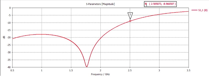
Figure 8: S11 parameter
The S21 parameter represents the insertion loss, that is, the power loss in transmission from port 1 to port 2. The loss is close to 0dB for lower frequencies and cut-off occurs at 2.5 Ghz beyond which the losses are higher. Thus the designed filter shows low pass response.
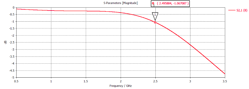
Figure 9: S21 parameter
Measurement Results
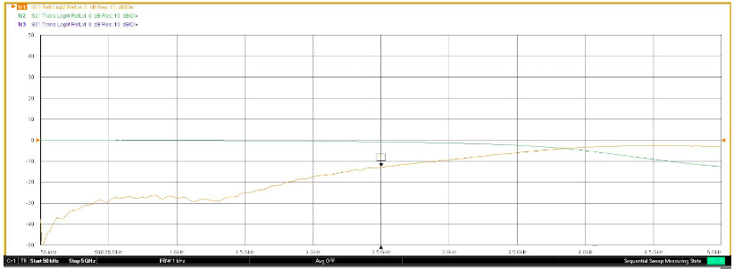
Figure 10: s-parameter analysis obtained from VNA
The S11 and S21 Parameters crossover point was obtained nearly at -3db Point.
In the results obtained from the VNA, the S11 parameter is indicated by the Yellow Line. The reflection/return loss value is well below -10dB for frequencies lower than 2.5 GHz and increases for higher frequencies. This implies that the cut-off for the filter is occurring close to 2.5GHz. This is in sync with the simulated values for reflection loss. The fabricated filter has more ripples in the passband as compared to the simulated one. These results are also reflected in the following table:
The S21 Parameter (Indicated by Green Line) represents insertion loss, for lower frequencies loss is very low, and cut-off occurs nearly at 2.5 GHz beyond which the losses are higher. But the transition from passband to stopband is slower compared to simulation results.
Applications
Chebyshev filters (type I) exhibit a fast transition between pass-band and stop-band but this is at the expense of an in-band ripple. The Chebyshev filter is still essential to many RF applications even though the in-band ripple may render some applications unfeasible. In order to significantly reduce undesirable out-of-band spurious transmissions like overtones or intermodulation, the steep roll-off is advantageously used. The optimal attenuation of undesirable signals can be obtained due to the quick transition between the pass-band and the stop-band.
Chebyshev filters (type II) do not have a ripple in the passband, that is, the passband is flat which makes them very useful for low frequency and DC measurement systems, such as bridge sensors, loadcells, etc.
Summary and Conclusion
In this report, we have designed a third-order Tchebyshev lowpass microstrip filter with a cut-off frequency of 2.5 GHz using CST Studio. All the calculations were performed using the mentioned standard formulas. After the verification of the design, the fabrication of the filter was done. The filter was then tested using the Vector Network Analyzer. From the return loss values, we observe that the cut-off frequency occurs at around 2.5 GHz, which is close to our desired result. The same can also be inferred from the insertion loss values. Thus, the results obtained for the designed filter match with the simulations in CST Studio.